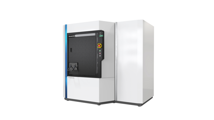
The PHI Genesis is the latest generation of PHI’s highly successful multi-technique XPS product line with PHI’s patented, monochromatic, micro-focused, scanning X-ray source.
It is an easy to use, fully automated system with auto-tuning and calibration and multiple parking positions for high throughput.
The fully integrated multi-technique platform of the PHI Genesis offers an array of optional excitation sources, sputter ion sources, and sample treatment and transfer capabilities. These features are essential in studying today’s advanced materials and in supporting your material characterization and problem-solving needs.
PHI Genesis offers high sensitivity and high throughput for large area and small area down to 5 µm and unique high-throughput non-destructive depth profiling using optional hard X-ray Cr source.
The instrument is fully customizable to address all analytical needs.
Intuitive Sample Navigation And Confident Analysis Area Identification
- The unique scanning X-ray microprobe allows SEM like navigation with point-and-click control
- X-ray induced secondary electron imaging (SXI) provides a perfect correlation between imaged areas and spectroscopy
- SmartMosaic for large-area SXI navigation and large area chemical mapping.
The Only Fully Automated High-Throughput Lab-Based Multitechnique XPS/HAXPES Instrument on the Market Commercially Available
- Large sample handling
- Multiple parking positions
- Automated sample transfer and handling
- Fast automated switching between XPS and HAXPES modes
Optimized Depth Profiling
- Multiple ion gun options (monatomic Ar, C60, argon cluster GCIB) for a variety of organic, inorganic, and mixed materials
- 4-axis stage functionality including rotation/tilt and heating/cooling during sputtering
- Multipoint profiling within a single sputter crater for on/off defect analysis and precious samples
- Adjustable solid collection angle for improved angular resolution for Angle-Resolved analysis with advanced software for high-throughput film structure analysis
Superior Micro-Area Analysis
- Highest small area sensitivity on the market
- <5 microns microprobe size in x and y for Al X-ray source and <14 microns for Cr X-ray source
- Image registration for unattended automated micro-area analysis
Bring HAXPES synchrotron capabilities into your lab with the PHI Genesis
- Analytical information depth using the Cr X-ray source is about 3 times deeper than with Al x-ray source
- Probing thicker film structures and buried interfaces, minimizing the effects of surface contamination and ion-induced chemical damage during depth profiling
Suite Of Specialized Solutions For In Situ Characterization Of Advanced Materials
- Electronic band structure of organic and inorganic materials using UPS, LEIPS, REELS measurement from the same sample location
- Electrochemical (biasing, polarization studies) experiments
- Inert sample transfer vessel
- Fully integrated high energy and high spatial resolution Auger Spectroscopy with elemental mapping at the exact location of interest as XPS
Capabilities of the PHI Genesis
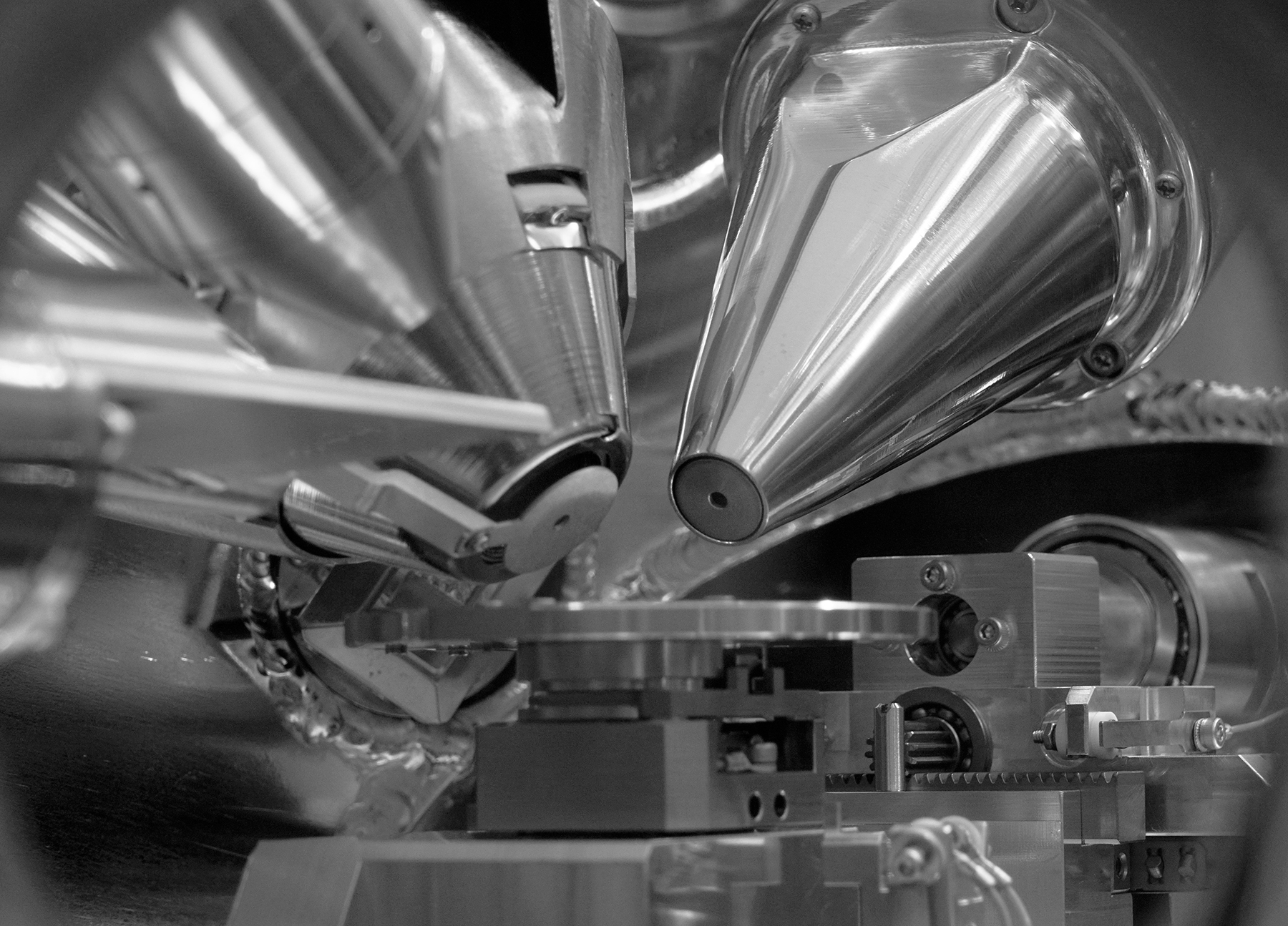
Micro-Focused Scanning X-ray Source and SEM-Like Operation
Ease of navigation and operation in SEM-like mode

SEM-Like XPS Microprobe
Unique CapabilitiesPHI’s scanning XPS microprobe instrument platform provides scanning X-ray induced secondary electron images (SXI) generated by scanning a focused sub-5 μm X-ray beam across the sample. Just like an SEM, SXI’s can be used to navigate to areas of interest and to select areas for analysis in real time. SXI images provide 100% confidence in locating small features of interest and in avoiding areas with contamination and inhomogeneities for analysis.
Smart Mosaic allows a user to set up a mosaic acquisition of SXI images from large areas. Stitched mosaic SXI images can be used to investigate the homogeneity of the sample across much larger areas
than available in a single SXI image.

High-Sensitivity Spectral and Imaging Analysis
A typical XPS analysis on the PHI Genesis begins by collecting an SXI image that is quickly generated using a sub-5 μm diameter raster scanned X-ray beam. Areas of interest for small or large spectral analysis or imaging are selected and used to guide the next steps which may include: obtaining high energy resolution spectra for chemical state analysis, chemical state images, or compositional sputter depth profiles.
Multispectral chemical maps can be acquired from areas of any size and stitched into a single large area chemical map. Overlays with a variety of color maps and transparency display options can be used to highlight areas that are spatially and chemically distinct.

Single Crater Multi-Point Depth Profiling
A powerful capability enabled by PHI’s unique scanning XPS microprobe technology is the ability to define analysis points on an SXI image and then obtain sputter depth profiles from multiple locations in a single sputter crater. For samples where sputtering area should be minimized, this is a powerful tool for analysis of neighboring features or on and off defect sites.
The image registration option is coupled to PHI’s unique SXI X-ray imaging capability to ensure XPS analysis is performed at the precise location of interest, even for very small features. Accurate positioning of very small features within a single sputter crater for analysis can be guaranteed.
Optimized Thin Film Depth Profile Analysis

Optimized Configuration
A focused X-ray beam, high sensitivity spectrometer, high performance floating column argon ion gun, automated dual beam charge neutralization, Zalar rotation, and advanced data reduction algorithms provides the highest performance XPS depth profiling capability available.
The standard monatomic argon ion gun can generate 5 eV to 5 keV Ar+ ion beams and is ideally suited for most inorganic depth profiling applications.

Argon Gas Cluster Ion Beam (GCIB) Option for Organic Depth Profiling
It is well known that monatomic Ar ion guns commonly used for inorganic thin film analysis typically cause severe chemical damage when sputtering most polymer and organic materials. PHI has led the way in developing and applying cluster source ion guns for the successful thin film analysis of polymer and organic materials. Our optional 20 kV Argon gas cluster ion beam (GCIB) and optional C60 ion gun have proven performance for depth profiling many polymer and organic films while minimizing the potential for chemical damage.


C60 Cluster Source Ion Gun Option for Mixed Matrix Depth Profiling
With the introduction of cluster source ion guns for organic and polymer thin film depth profiling, interest has grown in applying these ion guns to inorganic structures that sustain chemical damage with monatomic Ar ion beam sputtering. Our experience has shown that some metalloids, oxides, and thin film structures that contain both organic and inorganic materials sustain less chemical damage and differential sputtering artifacts when depth profiled using a 20 kV C60 cluster source ion gun.
Complete Electronic Band Structure Characterization

Measurement at the Same Location for XPS, UPS, LEIPS and REELS
In the PHI Genesis, LEIPS, UPS, Argon and GCIB ion beams, and neutralization beams are all aligned to the XPS measurement position. This allows for comprehensive evaluation of organic semiconductor materials.

Ultraviolet Photoelectron Spectroscopy (UPS) - Valence Band
Design of complex electronic material systems for display panels, flexible circuitry, and photovoltaics require knowledge of the basic properties of each component’s band structure in order to achieve efficient charge transport.
The combination of ultraviolet photoelectron spectroscopy (UPS) and low energy inverse photoemission spectroscopy (LEIPS) provides a complete characterization of the valence and conduction bands, as well as useful parameters such as the band gap, ionization energy, work function, and electron affinity.
Samples provided by: Organic Optoelectronics Practical Development Center(i3-opera)
Combined measurements from UPS and LEIPS
LEIPS provides accurate values of electron affinity (EA) which is required for designing organic light-emitting diode, understanding band structure at metal-semiconductor and heterojunctions and in studies of charge-transfer processes.semiconductor.
Low energy incident electrons (<5 eV) used in this technique are well-suited for analysis of organic materials with minimal damage.
The ionization energy can be obtained from the highest occupied molecular orbital (HOMO) of the UPS measurement. The electron affinity can be obtained from the lowest unoccupied molecular orbital (LUMO) of the LEIPS measurement. From the difference in those two values, the semiconductor bandgap energy can be calculated.
Combined measurements from UPS and LEIPS
- LEIPS is the inverse process of XPS/UPS
- A sample is irradiated with low energy (< 5 eV) electrons. Photons are emitted from the sample as electrons fill unoccupied states in the conduction band. Photon flux at fixed energy is measured relative to incident electron energy.
- Information obtained from LEIPS:
- Obtain information on the unoccupied electronic energy levels
- Measurement of the electron affinity of the sample
| Item | LEIPS |
A Conventional
Inverse Photoemission Spectroscopy |
| Analysis positions |
Same position as XPS, UPS, Ar/C60/GCIB ion guns, and AES/REELS | For dedicated IPES tool, sample transport required for XPS analysis |
| Energy or electrons |
≤ 5 eV Near ultraviolet Low Damage to organic material |
10 eV Vacuum ultraviolet Heavy sample damage |
| Selection of photon energy | Bandpass filter can be changed outside of bell jar | Bandpass filter is in an ultra-high vacuum chamber, difficult to replace |
| Energy Resolution |
≤ 0.45 eV |
0.6 eV |

Low Damage Analysis of Organic Matter
A comparison of the degree of electron beam damage on a thin film C60 sample using LEIPS electron energies and conventional IPES energies is shown. When the sample was irradiated with 10 eV electrons, equivalent to conventional IPES, the spectral shape changed, indicating that electronic damage had occurred. On the other hand, in the LEIPS measurement using 5 eV of electron energy, there is no change in the spectrum after extensive measurement time, suggesting that no sample damage has occurred.
Auger Electron Spectroscopy (AES)

When the features of interest are too small for XPS analysis, Auger Electron Spectroscopy (AES) is often used. The AES probe electron beam is up to 100 times smaller than the XPS X-ray beam, opening up new possibilities for sample characterization at increased spatial resolution.
With the PHI Genesis, the convergence of the optical, SXI, and SEM images allows for an intuitive approach to identifying regions of interest for analysis.
XPS and AES session tabs in the SmartSoft acquisition software are set up to operate seamlessly, allowing for in-situ analysis using both techniques at the same region of interest without moving the sample. Similar options for spectral analysis, depth profiling, line scans, and maps are available with both techniques.
Dual charge neutralization allows for AES analysis of insulating samples.
Reflection Electron Energy Loss Spectroscopy (REELS)

REELS capabilities
- Electronic state and bonding state of the surface
- Bandgap measurement of semiconductors
- Compare the relative hydrogen content of materials
- Observe evidence of conjugation/aromaticity in materials
- Discrimination of sp2 / sp3 bond of carbon

Hydridization Measurements by REELS for 2D materials
REELS is sensitive to the hybridization of carbon. Energy loss peak due to π-->π* transition in graphene appears 6-8 eV lower than the elastic peak.
Intensity of peak increases for higher sp2 character of carbon
Features of REELS
REELS measurement can be made by selecting one of the two electron guns as an option of PHI Genesis. Both electron guns can perform REELS measurement with high energy resolution of 0.5 eV or less according to FAT mode (constant energy resolution).
The first option for REELS is to get the "add-on" for the AES option by using the LAB6 electron gun as the source of energy. If the AES option is not available on your system, then second option for REELS is a newly developed, low-cost electron gun with a tungsten source is available.
Benefits of a Hard X-Ray Source
The Cr X-ray source has a photon energy of 5414.8 eV and provides for depths of analysis roughly 3 times those obtained using an Al X-ray source. This allows for:

Analysis of buried layers and interfaces deeper than traditional XPS
Si 2p high-resolution spectra obtained using Al and Cr X-Ray sources from a 25 nm SiO2 /Si sample. The signal from the Si metal substrate is detected in the spectrum obtained using the Cr source due to the larger information depth with respect to the Al source.

Decreased effect of chemical state damage induced by ion sputtering OR Elimination of Chemical State Damage at Interfaces
- Using the Cr X-ray source, quantitative depth profiles can be reliably obtained from ion-beam sensitive materials.
- Deeper sampling depth using the Cr source allows one to probe beyond the depth of possible damage induced by ion sputtering.
- A combination of Al and Cr data in depth profiles provides information on the extent of the damage.
Depth profile through a Pt overlayer on TiO2 using 500 eV Ar+. The Ti oxide spectrum obtained using the Al X-ray source shows clear damage, while the Ti oxide spectrum using the Cr X-ray source shows no sign of damage.

Reduced effect of surface contamination
An example of reduced sensitivity of Cr-based spectral data to adventitious contamination is demonstrated in the Figure below where two surveys from a contaminated vanadium substrate are overlaid. The zoom-in into the C 1s binding energy region shows a much higher relative intensity in the Al X-ray data source vs the Cr X-ray survey.
Alkα and Crkα surveys from staineless steel sample are overlaid. The zoom-in into C 1s binding energy region shows a much higher relative intensity in Alkα vs Crkα survey.

Access to additional transitions of higher binding energy for complementary chemical information and interpretation
Overlaid survey spectra of Ag foil collected with Al and Cr X-rays. Due to the higher photon energy of Cr X-rays, multiple higher binding energy transitions become available.

Lab-based HAXPES

Benefits over Synchrotron HAXPES
- Efficient charge neutralization for insulating and semiconducting samples
- Quantification of detected species
- Fast screening tool for experiment development before time-and cost-intensive synchrotron beam line testing
- Fully versatile and robust X-ray spectrometer using both soft and hard X-ray sources
- Fully versatile automation of switching between Al and Cr sources (approximately 1 minute switchover time) and robust X-ray spectrometer using both soft and hard X-ray sources
- High throughput spectrometer with all data acquisition capabilities for both X-ray sources
- Full automation of sample manipulation and data acquisition
- Large sample mount with 2 additional parking positions
Efficient charge neutralization: left - high-resolution C 1s from PET shows excellent chemical state separation using both sources; right – XPS and HAXPES Si 2p and O 1s from SiO2 overlaid showing the symmetrical shape and similar width of spectra.
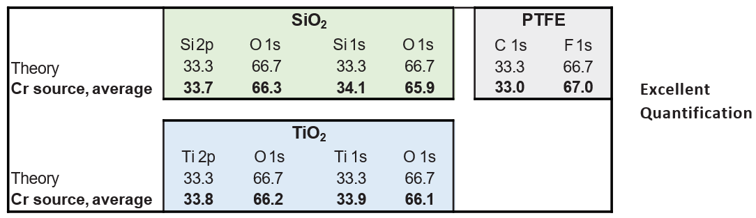
- Quantification using theoretical relative sensitivity factors for reference bulk materials using low and high binding energy transitions.
Benefits of Combining XPS with HAXPES
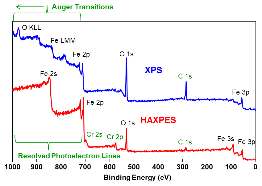
Collecting spectra from the same sample using both Al Kα and Cr Kα X-ray sources demonstrates the ability to shift Auger transitions and clearly resolve overlapped photoelectron lines.
In the survey spectrum obtained from a stainless steel sample with Al X-rays (blue trace), the Fe and O Auger transitions overlap with photoelectron lines. Using the Cr X-ray source (red trace) the Auger peaks are shifted and the photoelectron lines can be resolved. Of note: Because of the larger analysis volume of HAXPES, the C 1s peak is much smaller in the HAXPES spectrum, compared to the XPS spectrum.

HAXPES is much less surface sensitive than XPS, reducing the need to clean adventitious contamination prior to analysis.
Chemical information from both surface (XPS) and near-surface (HAXPES) depths can be obtained without ion beam sputtering.
High-resolution Fe 2p and Cr 2p spectra using Al (blue) and Cr (red) X-ray sources show oxidation at the surface and a mixture of oxides and metals at deeper depths.
MultiPak Data Reduction Software

Data Reduction for XPS and AES
PHI MultiPak is the most comprehensive data reduction and interpretation software package available for electron spectroscopy. The tasks of spectral peak identification, extracting chemical state information, quantification, and detection limit enhancement are addressed with an array of powerful and easy-to-use software tools for spectra, line scans, images and sputter depth profiles. MultiPak can be used on the instrument PC to process data in real time or on an off line PC for report generation.
Advanced Data Reduction Tools
- Auto peak identification
- XPS chemical state database
- XPS spectral deconvolution
- Quantitative analysis
- Non-linear least squares fitting
- Linear least squares fitting
- Target factor analysis
- Retrospective chemical imaging
- Batch mode data processing
Brochures
PHI HAXPES User Group
Application Notes
What Our Customers Say
“The PHI Genesis X-ray Photoelectron Spectroscopy (XPS) instrument has revolutionized our lab's capabilities. Its advanced features and flexibility enable detailed surface material analysis, while PHI's exceptional support ensures smooth operations. The seamless installation and insightful training provided by PHI's knowledgeable field engineers have made this system an invaluable addition to our facilities.”
Quantum Valley Ideas Lab
“PHI's service team is exceptional. Their engineers are professional, reliable, and knowledgeable, always seeking help when needed to ensure reliability. The scientists are equally impressive, providing clear guidance for analysis. PHI's customer service is amazing.”
NY CREATES
“As a global supplier in the automotive, aerospace, and industrial markets, we rely on PHI Auger instruments for customer support, production, and R&D. The PHI 710 Auger, with its state-of-the-art capabilities and excellent customer support, continues to drive our product and process development. The expertise of PHI's service engineers and scientists, along with the flexibility to add specific capabilities, strengthens our long-standing relationship with PHI.”
Manufacturing Customer
“PHI's prompt and willing responses to our VersaProbe system and data analysis concerns have been invaluable. Their excellent application support ensures we always have the help we need.”
University of Virginia
“PHI's TOF-SIMS studies were instrumental in resolving a major issue in our products. Their expertise helped us identify the compromised film, enabling us to successfully address the problem. PHI's support was a significant contributor to our success.”
Semiconductor Contract Customer
Previous Next“We are very pleased with the timely assistance our users have received from PHI's application department over the past six years. The experienced application scientists provide invaluable tips and share application materials promptly, often on the same day. PHI's support has been crucial in expanding our user base and exploring new applications on the system.”
Seagate
Learn how our instruments can help with your applications