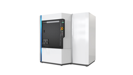
Fully automated multi-technique scanning XPS/HAXPES microprobe
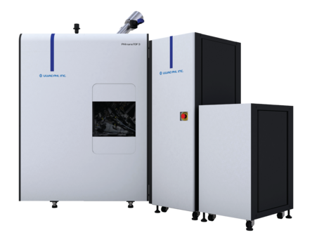
A TOF-SIMS instrument optimized for the highest sensitivity elemental and molecular analysis
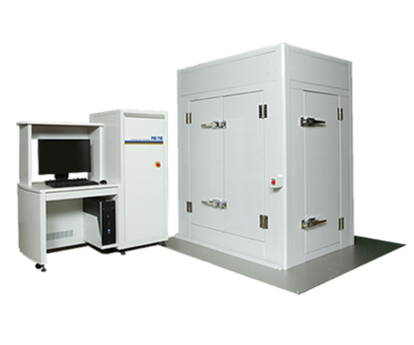
A high precision Sims analysis tool for automated depth profiling
A scanning Auger instrument optimized for high magnification chemical imaging
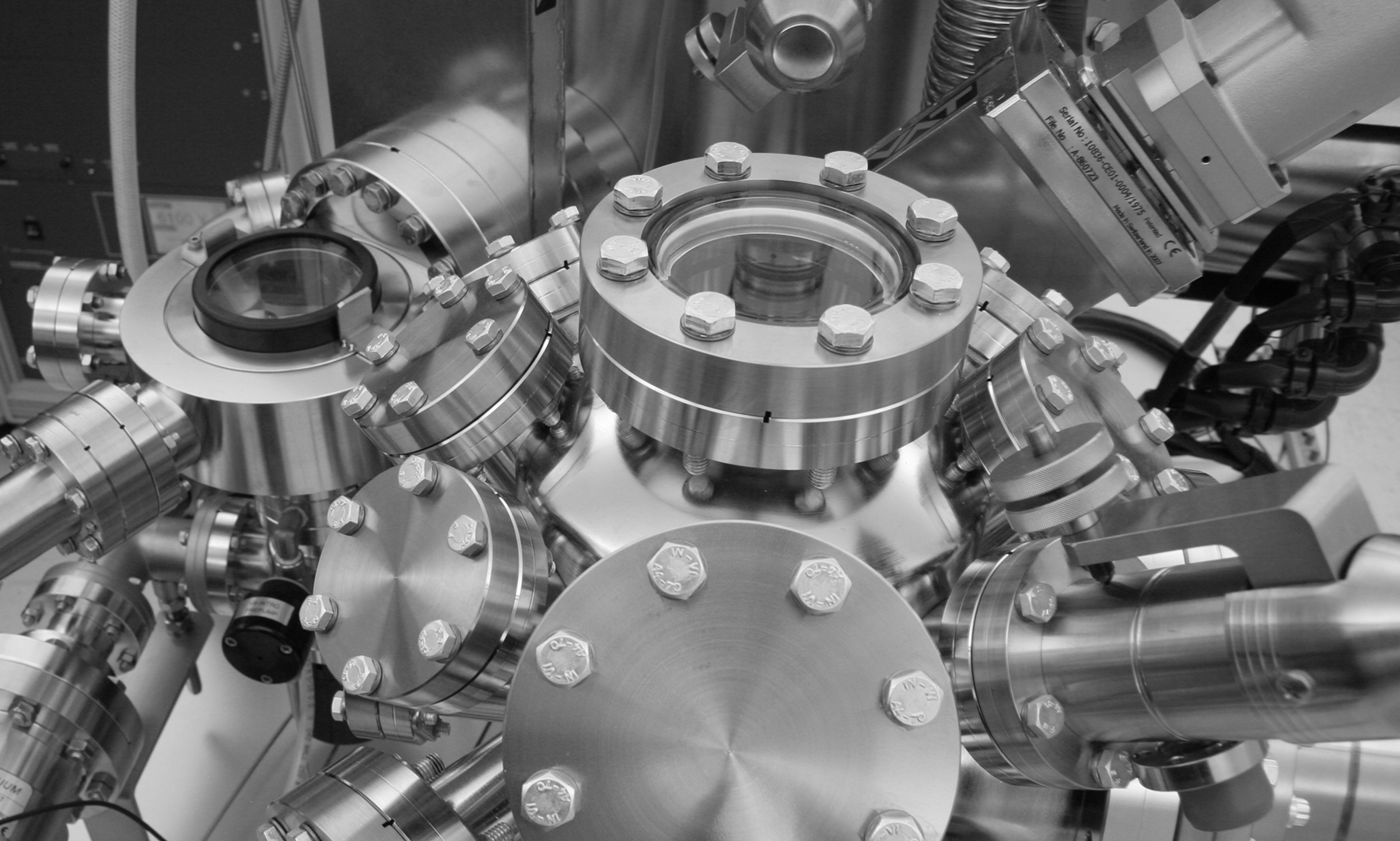
These instruments have been fully refurbished at PHI and performance has been brought up to the original specifications.
A list of field upgrades currently available for your system.
A list of software currently available for your system.