AES Surface Analysis
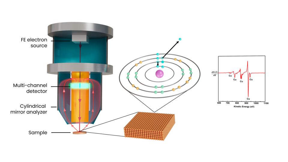
Achieve SEM-like ultra-high resolution elemental materials characterization with the PHI 710 Scanning Auger Nanoprobe, a premier tool for nanometer-scale surface and thin film analysis. Auger electron spectroscopy (AES) via the PHI 710 enables precise identification of elemental composition – ideal for advanced materials research and failure analysis, delivering detailed insights critical for innovation in semiconductors, nanotechnology and materials science.
Learn more about the AES technique.
Available AES Analytical Services
- Quantitative elemental spectroscopy and nanoscale surface imaging up to 10 nm below a material’s surface, which allows for probing film structures and buried interfaces
- Sub-10 nm spatial resolution for elemental mapping and SEM-like imaging—down to 8 nm for AES maps and 3 nm for secondary electron images
- Nanoscale alternative to SEM-EDS (energy dispersive X-ray spectroscopy), offering superior surface sensitivity and compositional information
- Inert sample transfer for air-sensitive materials
- Monoatomic argon (Ar⁺) sputter depth profiling for compositional analysis through layered structures
Example AES Output – Nanoscale Elemental Analysis of Particle

A 500-nm particle is presented in a high-resolution SEM-AES image (left) and a corresponding Auger Elemental Map (right) of a 1 µm × 1 µm field of view. The SEM-AES image provides detailed surface morphology, while the elemental map reveals the spatial distribution of key elements: copper (green), manganese (blue), oxygen (red), oxidized copper (yellow), and oxidized manganese (magenta) with iron also identified in the surrounding matrix. This analysis was performed using the PHI 710 Auger Nanoprobe, leveraging its exceptional surface sensitivity, nanoscale spatial resolution, and the ability to detect and map elemental compositions with high precision. These capabilities make it ideal for advanced materials characterization, particularly in identifying surface composition and contaminants at the nanoscale.
PHI 710 Scanning Auger Nanoprobe
- Maximum sample size of 60 mm diameter and 20 mm thickness
- Maximum electron beam accelerating voltage of 25 kV
- Sample must be a solid and compatible with ultra-high vacuum (no liquid)

PHI 710 Scanning Auger Nanoprobe
Working Principle of AES Technique
Learn more about the AES technique.