XPS/HAXPES Surface Analysis
Unlock detailed surface and subsurface insights with PHI’s advanced X-ray photoelectron spectroscopy (XPS) and hard X-ray photoelectron spectroscopy (HAXPES) capabilities. Our PHI Quantes XPS/HAXPES Scanning Microprobe instrument delivers high-resolution elemental and chemical-state information from up to 10 nanometers below a material’s surface, and up to 30 nanometers with HAXPES.
With dual X-ray sources (Al Kα and Cr Kα) and integrated sputter ion guns, we offer both non-destructive and destructive depth-profiling analysis for complex film structures and buried interfaces.
Learn more about the XPS and HAXPES techniques.
XPS and HAXPES Analytical Services
- Quantification of elements and chemical states of up to 10 nm (XPS) and 30 nm (HAXPES) below a material’s surface
- Angle-resolved analysis for non-destructive multi-layer film thickness measurement (AR-XPS and AR-HAXPES)
- Inert sample transfer for air-sensitive samples
- Monoatomic argon (Ar+) sputter depth-profiling for compositional analysis through layered structures
- Argon gas cluster ion beam (GCIB) cleaning for surface contamination removal
- GCIB depth-profiling optimized for organics, inorganics, and hybrid materials
Example XPS Output – Thin Film Thickness on Medical Device

A small area on a wire-mesh medical device was analyzed using a PHI XPS/HAXPES scanning microprobe as shown by X-ray beam scan line in the SEM-like scanning X-ray image on the left. The top right graph displays high-resolution XPS spectra for carbon, titanium, and nickel, identifying chemical states such Organic carbon, oxidized titanium, and metallic nickel were identified in the respective high-resolution XPS spectra.
The bottom right plot illustrates a non-destructive XPS depth profile from with advanced thin-film analysis software StrataPHI, revealing an organic coating (6.4 nm), a thin TiO₂ layer (0.4 nm), and the underlying NiTi substrate. PHI XPS instruments enable precise chemical-state identification and quantitative depth analysis with high spatial resolution, making it ideal for surface characterization of complex layered materials and thin films.
Example HAXPES Output – Buried Layer in Semiconductor Device
The figure illustrates a multilayer silicon wafer structure composed of an 8 nm HfO₂ overlayer and an 8 nm buried SiO₂ layer. The top right graph shows a conventional XPS spectrum of Si 2p acquired using Al Kα X-rays where only a small Si-O signal from the buried SiO₂ layer is visible. The Si substrate remains undetected due to the high surface sensitivity of XPS.
In contrast, the bottom left HAXPES spectrum of Si 1s collected using Cr Kα X-rays reveals both the Si-O signal from the buried SiO₂ layer and the Si-Si signal from the underlying silicon substrate, demonstrating enhanced depth sensitivity. The bottom right HAXPES spectrum of Hf 3d5/2 confirms the presence of Hf-O in the HfO2 layer. This comparison highlights the complementary strengths of HAXPES and traditional XPS, combining the deep interface analysis via HAXPES with the high surface sensitivity of XPS for non-destructive characterization of complex thin-film structures.

PHI Quantes Scanning XPS/HAXPES Microprobe
- Analysis area up to 1350 µm x 1350 µm
- Selectable X-ray beam size between 7.5 µm and 200 µm
- Maximum sample size of 75 mm x 75 mm x 20 mm
- Sample must be a solid and compatible with ultra-high vacuum (no liquid)
- Sample tilting from 5º to 90º take-off angle for grazing-angle analysis and subsurface depth-profiling

PHI Quantes XPS/HAXPES Scanning Microprobe
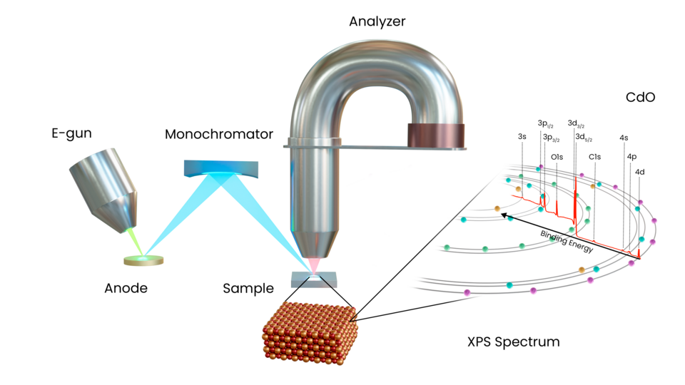
Working Principle of XPS Technique