X-ray Photoelectron Spectroscopy (XPS) also known as Electron Spectroscopy for Chemical Analysis (ESCA) is the most widely used surface analysis technique because it can be applied to a broad range of materials and provides valuable quantitative and chemical state information from the surface of the material being studied. The average depth of analysis for an XPS measurement is approximately 5 nm. PHI XPS instruments provide the ability to obtain spectra with a lateral spatial resolution as small as 7.5 µm. Spatial distribution information can be obtained by scanning the micro focused x-ray beam across the sample surface. Depth distribution information can be obtained by combining XPS measurements with ion milling (sputtering) to characterize thin film structures. The information XPS provides about surface layers or thin film structures is important for many industrial and research applications where surface or thin film composition plays a critical role in performance including: nanomaterials, photovoltaics, catalysis, corrosion, adhesion, electronic devices and packaging, magnetic media, display technology, surface treatments, and thin film coatings used for numerous applications.
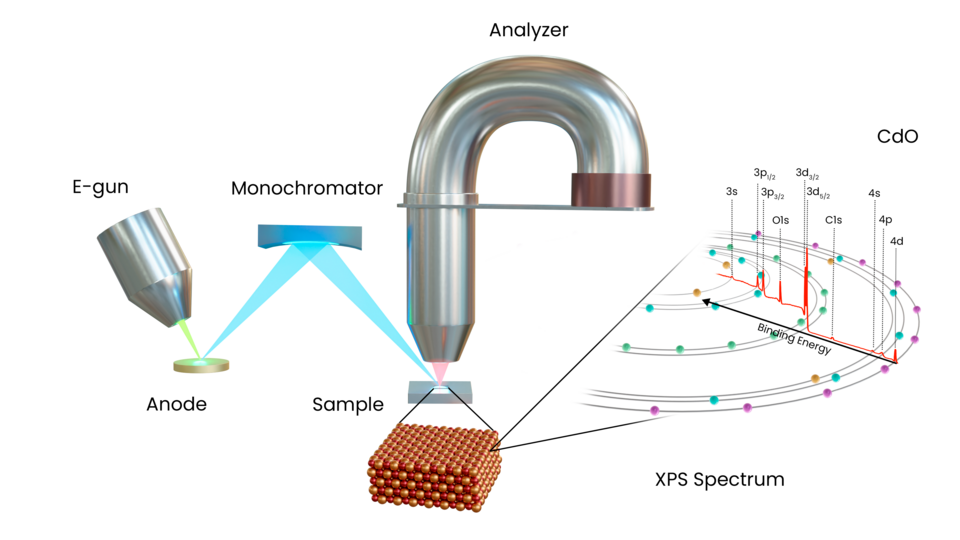
XPS is typically accomplished by exciting a samples surface with mono-energetic Al kα x-rays causing photoelectrons to be emitted from the sample surface. An electron energy analyzer is used to measure the energy of the emitted photoelectrons. From the binding energy and intensity of a photoelectron peak, the elemental identity, chemical state, and quantity of a detected element can be determined.
Physical Electronics XPS instruments function in a manner analogous to SEM/EDS instruments that use a finely focused electron beam to create SEM images for sample viewing and point spectra or images for compositional analysis. With the PHI XPS instruments, a finely focused x-ray beam is scanned to create secondary electron images for sample viewing and point spectra or images for compositional analysis. The size of the x-ray beam can be increased to support the efficient analysis of larger samples with homogeneous composition. In contrast to SEM/EDS which has a typical analysis depth of 1-3 µm, XPS is a surface analysis technique with a typical analysis depth of less than 5 nm and is therefore better suited for the compositional analysis of ultra-thin layers and thin microscale sample features.