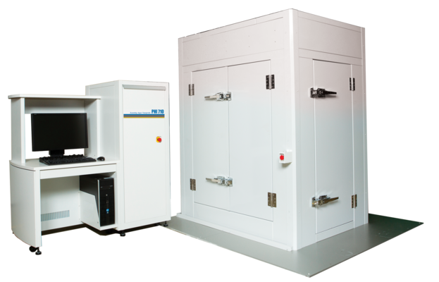

The PHI 710 Scanning Auger Nanoprobe is a unique, high performance Auger Electron Spectroscopy AES instrument that provides elemental and chemical state information from sample surfaces and nano-scale features, thin films, and interfaces. Designed as a high performance Auger, the PHI 710 provides the superior Auger imaging performance, spatial resolution, sensitivity, and the spectral energy resolution needed to address your most demanding AES applications.
Unique Technology
- Coaxial electron gun and analyzer geometry provides the sensitivity and unobstructed vision needed to fully characterize the microstructures that exist on most real-world samples.
- Auger data is obtained from all sides of particulates and between particles with equally high sensitivity providing Auger maps with meaningful compositional information.
- Imaging of textured or curved samples without analyzer induced shadowing
Superior Auger Imaging
- High performance electron optics, precision sample handling, and advanced vibration and thermal isolation provide a superior environment for nano-scale Auger imaging and analysis
- Working magnifications of 500,000 X and higher
- Robust mage registration for unattended automated micro-area analysis
Nanoscale Thin Film Analysis
- Floating column ion gun provides a broad range of depth profiling capabilities
- Higher ion beam energies (2-5 keV) allow structures several microns thick can be routinely depth profiled
- The use of lower accelerating voltages reduces sputter mixing that could broaden the observed interfaces in an ultra thin (<5 nm) film structure
Modern, Easy To Use Software Platform
- Intuitive, fully integrated, Windows™ software platform controls all instrument functions
- Session tabs guide you through the analysis process
- Seamless interface to PHI MultiPak, the most comprehensive data reduction and interpretation software package available for electron spectroscopy
Multiple Optional Technique Add-ons And Accessories For Specialized Experiments
- Liquid metal focused ion beam (FIB) allows for in-situ cross-sectioning of particles, defects and coatings
- Energy Dispersive X-ray Spectroscopy (EDS) detector provides information about elemental qualitative and quantification. The windowless software driven motor-controlled detector has a short working distance for wide acceptance angles
- Backscattered Electron Detector (BSE) provides topographic information and compositional information of the sample by using a four-quadrant detector.
- Electron Backscatter Diffraction (EBSD) detector provides information about crystal structure and grain orientation
Microstructure Analysis on Real World Samples
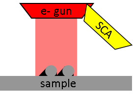
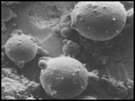
Coaxial Analyzer / Electron Gun Geometry
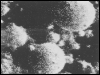
PHI’s coaxial electron gun and analyzer geometry provides the sensitivity and unobstructed vision needed to fully characterize the microstructures that exist on most real world samples with Auger Electron Spectroscopy. In this example, Auger data is obtained from all sides of particulates and between particles with equally high sensitivity.
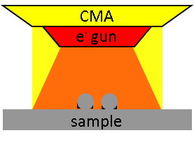
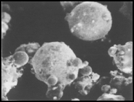

- Cylindrical Mirror Analyzer (CMA) with coaxial field emission electron gun
- Imaging of textured or curved samples without analyzer induced shadowing
- High sensitivity at all sample tilt angles
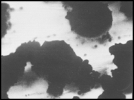
Non-Coaxial Analyzer / Electron Gun Geometry
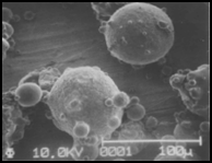
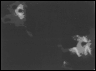
Instruments with non-coaxial geometry suffer from geometric effects that dramatically reduce instrumental sensitivity and even create shadows that prevent any analysis in some locations. In this example high sensitivity is only observed on areas of the particles that face the analyzer, while the back side of the particles and the areas between particles are inaccessible because of analyzer shadowing that occurs in an instrument with non-coaxial geometry.
Nanoscale Thin Film Analysis
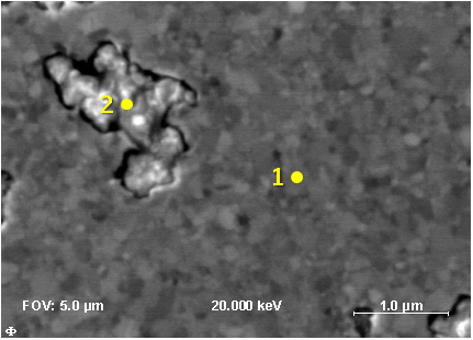
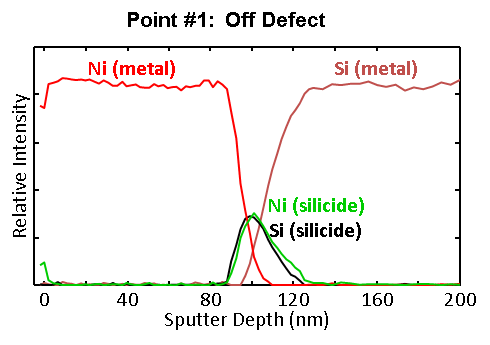
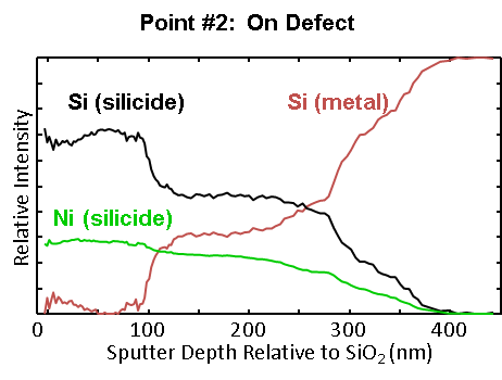
The sample shown in the SEM image contains a defect that appeared in a thin nickel film deposited on a silicon substrate after it was annealed to form a nickel silicide at the interface. Multi-point depth profiles obtained with a 20 nm diameter electron beam for analysis and a 500 V Ar ion beam for sputtering were acquired using high energy resolution (0.1%) on and off of the defect. Linear least squared fitting software was used to isolate the Ni metal and Ni silicide spectra as well as the Si metal and silicide spectra. It can be noted that Ni silicide is found only at the interface and not in the Ni film or in the Si substrate at point 1, which is off of the defect. However, in the defect area at point 2 a complex multi-phase Ni silicide is observed throughout the defect in the Ni coating.
Superior Auger Imaging
The secondary electron image in figure A shows the microstructure of a ductile iron fracture surface including graphite nodules and craters where graphite nodules have fallen out as a result of the fracture. The AES maps in figure B show the ability to map across the graphite nodule and the crater where Sn has segregated to the nodule/iron interface. The SE image and AES maps in figures C and D show the complex composition of a small precipitate observed in figure B. Only PHI Auger instruments with coaxial electron gun and analyzer geometry provide such a complete compositional picture of a micro-structured sample surface.
- CMA with coaxial electron gun
- High stability analysis platform
- Robust image registration software

, C (blue), and Sn (yellow)")

, Ca (blue), and Ti (red)")
SmartSoft-AES
- Intuitive, fully integrated, Windows™ software platform controls all instrument functions.
- Session tabs guide you through the analysis process
- Seamless interface to PHI MultiPak data reduction software
MultiPak Data Reduction Software
PHI MultiPak is the most comprehensive data reduction and interpretation software package available for electron spectroscopy. The tasks of spectral peak identification, quantification, extracting chemical state information, detection limit and image enhancement are addressed with an array of powerful and easy-to-use software tools for spectra, line scans, images and depth profiles.
Color overlay of elemental silicon (green), silicide (red) and silicon oxynitride (blue) images created using the Linear Least Squares fitting algorithm in MultiPak to extract multiple silicon chemical state images from the elemental silicon image.
Brochures
Application Notes
What Our Customers Say
“The PHI Genesis X-ray Photoelectron Spectroscopy (XPS) instrument has revolutionized our lab's capabilities. Its advanced features and flexibility enable detailed surface material analysis, while PHI's exceptional support ensures smooth operations. The seamless installation and insightful training provided by PHI's knowledgeable field engineers have made this system an invaluable addition to our facilities.”
Quantum Valley Ideas Lab
“PHI's service team is exceptional. Their engineers are professional, reliable, and knowledgeable, always seeking help when needed to ensure reliability. The scientists are equally impressive, providing clear guidance for analysis. PHI's customer service is amazing.”
NY CREATES
“As a global supplier in the automotive, aerospace, and industrial markets, we rely on PHI Auger instruments for customer support, production, and R&D. The PHI 710 Auger, with its state-of-the-art capabilities and excellent customer support, continues to drive our product and process development. The expertise of PHI's service engineers and scientists, along with the flexibility to add specific capabilities, strengthens our long-standing relationship with PHI.”
Manufacturing Customer
“PHI's prompt and willing responses to our VersaProbe system and data analysis concerns have been invaluable. Their excellent application support ensures we always have the help we need.”
University of Virginia
“PHI's TOF-SIMS studies were instrumental in resolving a major issue in our products. Their expertise helped us identify the compromised film, enabling us to successfully address the problem. PHI's support was a significant contributor to our success.”
Semiconductor Contract Customer
Previous Next“We are very pleased with the timely assistance our users have received from PHI's application department over the past six years. The experienced application scientists provide invaluable tips and share application materials promptly, often on the same day. PHI's support has been crucial in expanding our user base and exploring new applications on the system.”
Seagate
Learn how our instruments can help with your applications