Driving Discoveries Through Surface Analysis
Physical Electronics (PHI), the premier name in surface analysis, offers one-stop surface analytical services and materials testing using our state-of-the-art instruments located in a same facility. Our scientists have a deep knowledge of surface analysis applications and problem solving, and the benefit of always having access to the latest instrumentation technology. It is a winning combination to help you tackle your most challenging production, R&D, and engineering issues.
To discuss a particular project or to request a quote, please email us at analysis@phi.com or call us at 518-650-1892 (8 a.m.-5 p.m. CST)
Common Applications
|
|
Surface Analysis Techniques
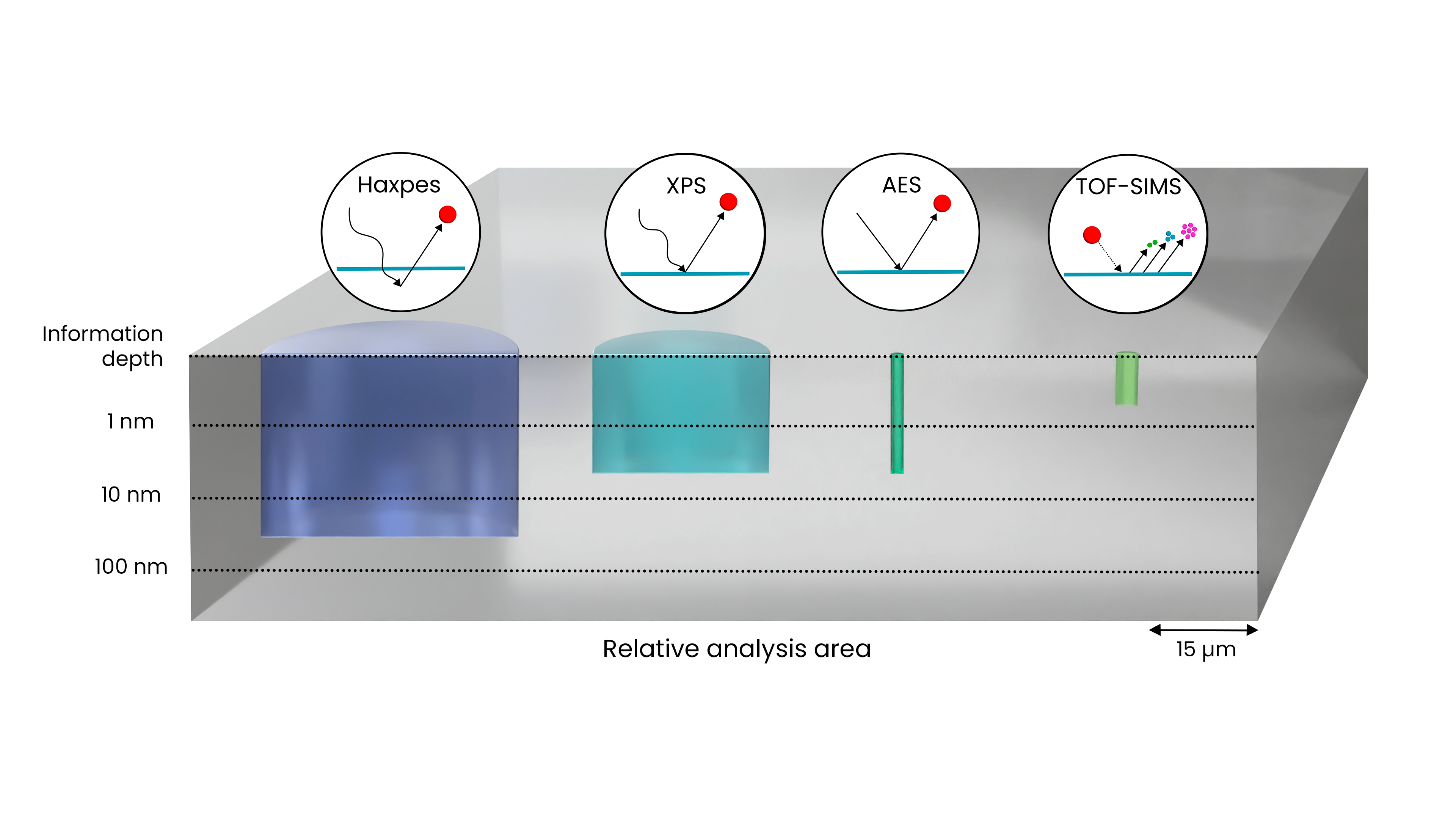
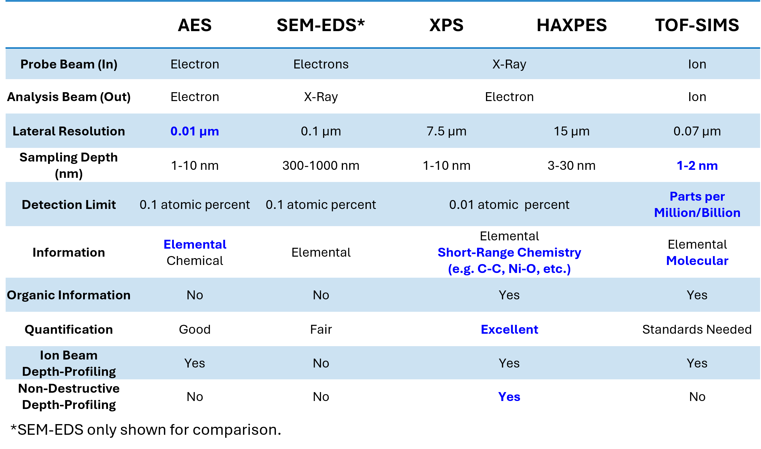
XPS/ESCA/HAXPES
X-ray photoelectron spectroscopy (XPS) surface analysis instruments provide elemental and chemical state information by measuring the binding energy of photoelectrons that have been excited with a mono-energetic x-ray beam. With the use of a sputter ion gun to remove material, thin film depth profile characterization is also possible.
Learn moreTOF-SIMS
PHI's time-of-flight secondary ion mass spectrometry (TOF-SIMS) surface analysis equipment provides elemental, chemical and molecular information by measuring the mass of ions that have been ejected from a sample's surface with the use of a focused ion beam.
Learn moreAES
Our Auger electron spectroscopy (AES) surface analysis equipment provides elemental and in some instances chemical information with the use of a finely focused electron beam to excite the Auger electrons. The analysis of submicron features is routine and thin film depth profile analysis is possible with the use of a sputter ion gun to remove material.
Learn more