
𝗦𝗵𝗼𝗿𝘁 𝗮𝗻𝘀𝘄𝗲𝗿. Wide-bandgap semiconductor performance depends on interfaces, contacts, and processed surfaces. Electrical tests alone cannot identify the chemistry of these features. PHI surface analysis instruments identify chemical changes at semiconductor surfaces and interfaces. XPS/HAXPES measures chemical states in gate stacks and at buried interfaces. Scanning AES determines the elemental composition of small interconnect features. TOF-SIMS with tandem MS maps residues and identifies their molecular composition. The appropriate technique depends on the layer stack, the feature size, and the question that process or device data have left unresolved.
Key takeaways
- XPS and HAXPES reveal chemical states at wide-bandgap surfaces and selected buried interfaces, so you can compare the effects of deposition, cleaning, or annealing.
- Scanning AES isolates the elemental chemistry of small contacts and defects, helping you distinguish a local surface problem from nearby material.
- TOF-SIMS imaging and tandem MS locate trace residues and test their molecular identity when an elemental map leaves the source unclear.
Which problem are you trying to solve?
| Customer question | Measurement | Information gained |
|---|---|---|
| Did processing change the surface or buried interface? | XPS and HAXPES | Composition and chemical states of the interface |
| Is a defect limited to a small contact or feature? | Scanning AES / small-area XPS with SXI | Local surface elements compared with surrounding material |
| What trace residue remains after patterning? | TOF-SIMS tandem MS | Species distribution and fragmentation evidence for molecular assignment |
Performance tests characterize the behavior of devices and interconnects, while imaging and mapping identify the locations of relevant features. Spectroscopic surface analysis provides complementary chemical information. Comparing affected and reference samples under the same analytical conditions helps establish relationships between measured chemical differences, process history, and device performance.
These characterization questions arise throughout wide-bandgap semiconductor development, including GaN and SiC programs. The published examples below illustrate how surface analysis addresses such questions in semiconductor integration structures.
Examples from semiconductor workflows
Gate dielectric interfaces
Buried gate chemistry in GaN power devices
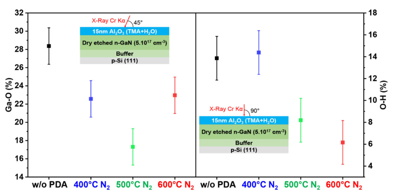
Post-deposition annealing changes the chemistry of the Al₂O₃/GaN interface in a GaN MOS-channel high-electron-mobility transistor. The PHI Genesis combines Al Kα XPS with optional Cr Kα HAXPES in a single scanning microprobe, enabling analysis of the same selected area at complementary information depths.
Conventional Al Kα XPS typically probes the upper 5–10 nm of a material. Cr Kα HAXPES provides approximately three times greater information depth, enabling acquisition of Ga 2p and O 1s spectra from the buried Al₂O₃/GaN interface without removing the overlying oxide by ion sputtering, which can alter the chemistry being investigated. The information depth and sensitivity to the buried interface depend on the material, photoelectron transition, film thickness, and measurement geometry.
In a published device study using a PHI XPS/HAXPES instrument:
- HAXPES identified Ga–O bonding at the Al₂O₃/GaN interface and hydroxyl (OH) contributions in the oxide.
- The contribution from interfacial gallium oxide decreased as the annealing temperature increased to 500 °C.
- The study linked these chemical changes to reduced electrical hysteresis.
These measurements help process engineers relate annealing-induced changes in interface chemistry to device performance, providing chemical evidence beyond the correlation between annealing temperature and electrical behavior. Read the GaN HAXPES example →
Small interconnect features
Local chemistry on an isolated solder bump
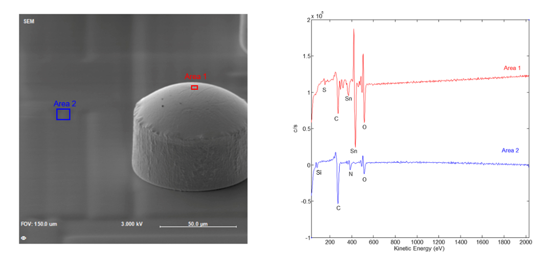
In heterogeneous integration, small amounts of contamination on a solder bump can alter the contact surface. Scanning Auger electron spectroscopy (AES) measures the near-surface elemental composition of a selected micro-area. In a PHI 710 analysis of an electrically isolated Sn solder bump, AES detected Sn, C, O, and trace S on the bump. The surrounding polyimide exhibited a distinct elemental composition. The analysis conditions were selected to avoid charging artifacts.
These measurements identify localized oxygen and potential residues, providing chemical evidence for further failure analysis. AES alone does not establish that sulfur or carbon caused poor wetting, high contact resistance, or device failure in service. Establishing that relationship requires process history and supporting electrical measurements or other corroborating evidence.
For smaller patterned features, AES imaging and depth profiling of a semiconductor via demonstrate how elemental distributions can be examined both laterally and as a function of depth within a selected structure.
Patterned structures
Molecular identity of sidewall residues
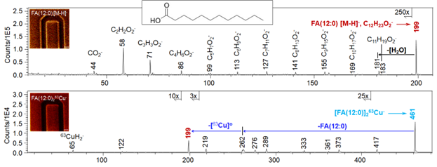
AES can locate carbon on a patterned feature but generally cannot identify the organic molecule from which it originates. In a PHI NanoTOF TOF-SIMS tandem MS imaging study, investigators examined carbon-containing residues on lithographically patterned and etched structures. Tandem mass spectra identified two fatty acid contaminants, FA(12:0) and FA(16:0), on the sidewalls. The study also associated higher-mass signals from Cu-plated regions with copper–fatty acid complexes.
This molecular information supports process investigations by extending the analysis beyond the location of carbon contamination. Molecular fragments and isotope patterns help identify the likely chemical nature of the residue and characterize its interaction with Cu.
How to choose your technique
Use XPS to determine chemical states at accessible surfaces. Use HAXPES when the relevant interface lies beneath a film but remains within the information depth of the method. Use AES when the question concerns the elemental composition of a small contact, particle, or patterned feature. Use TOF-SIMS when trace species, molecular identity, or their spatial distribution is central to the investigation. Correlate the chemical results with process splits and device data before assigning a failure mechanism.
| Method | Best fit | Check before testing |
|---|---|---|
| XPS / HAXPES | Chemical states at a surface or buried interface | Overlayer thickness, core-level transition, measurement geometry, and expected interface signal |
| Scanning AES | Elemental composition of small contacts or patterned features | Charging, beam sensitivity, and sample accessibility |
| TOF-SIMS tandem MS | Distribution of trace residues and assignment of their molecular identity | Reference ions, matrix effects, and quantitative controls |
Frequently asked questions
Can HAXPES measure a buried interface without sputtering?
Yes, provided that the overlayer thickness and the selected photoelectron transition allow a measurable interface signal. Cr Kα HAXPES probes approximately three times deeper than conventional Al Kα XPS. Information depth depends on both the sample and the transition, so it should be verified for the actual layer stack.
When should I use AES instead of XPS for a semiconductor defect?
Use scanning AES when the target is a very small feature and the main question is which elements are present at its surface. Use XPS when chemical states and more quantitative composition are the priority and the feature is large enough for the selected X-ray analysis area.
What does TOF-SIMS tandem MS add to an elemental map?
An elemental map can locate carbon but cannot identify the organic residue. Tandem MS fragments a selected ion to test a molecular assignment, and TOF-SIMS imaging shows where that species occurs. Concentration claims should be confirmed with appropriate standards.
If you have a problem involving a GaN gate stack, an interconnect, or a patterned residue, contact PHI. Please provide the layer structure, the feature size, the suspected species, and the comparison you need to make.
Contact PHI Contact PHI